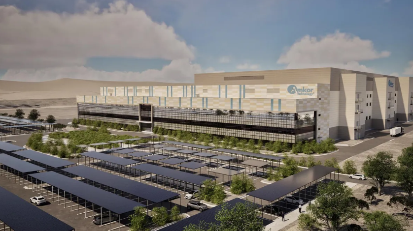
Amkor Technology is super-charging its U.S. footprint in Peoria, Arizona, lifting the investment for its advanced semiconductor packaging and test campus to $7 billion across two phases. The plan calls for roughly 750,000 square feet of cleanroom space, with construction of the first factory wrapping in mid-2027 and production starting in early 2028. The move follows Amkor’s site shift to a larger parcel in North Peoria and a groundbreaking earlier this month.
For manufacturing teams, this isn’t just another ribbon-cutting. Advanced packaging lives and dies by stable thermal steps. Lines like these run on substrate dry, die-attach bake, underfill cure, post-mold cure, and a final bake-out before test. As devices stack more dies and push higher power, temperature uniformity, tight ramp/soak profiles, and cleanroom-ready ovens become key yield levers. A campus of this size signals fresh demand for precise, repeatable heat treatment in the U.S. – close to wafer fabs and system makers that need fast turns.

The Arizona location matters too. Phoenix has quickly grown into a chip corridor, and keeping packaging nearby shrinks logistics risk and shortens WIP cycles. Amkor and state officials say the build will support thousands of skilled jobs while anchoring domestic capacity for AI, automotive, and high-performance computer programs.
For process engineers and QA leaders, the timeline offers a planning runway: tool specs and validation windows can be mapped now to hit the 2028 start of production.
Looking ahead, watch the tool awards that follow. Decisions on package types and materials – substrates, adhesives, encapsulants – will set thermal budgets for each line. That flows straight into oven zoning, airflow design, and energy use targets that plant managers juggle every day.
Article & Image source Amkor Technology – Official Website