Curing ovens provide a controlled environment that manufacturers can use in advanced chip packaging. Typical semiconductor applications where curing ovens play a critical role are:
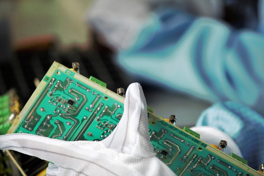
- Baking and Curing of Adhesives and Sealants: Industrial ovens are used for baking and curing adhesives and sealants in chip packaging. These adhesives are essential for bonding the semiconductor die (the actual microchip) to the packaging substrate or lead frame. The oven provides controlled heat and temperature profiles to ensure proper curing, resulting in strong and reliable bonds.
- Solder Reflow: In surface mount technology (SMT) and through-hole technology (THT) used in chip packaging, solder reflow ovens are employed. These ovens heat the solder paste applied to the circuit board, allowing it to melt and create secure electrical connections between the chip’s leads or pads and the circuit board. This process is critical for attaching the chip to the board during assembly.
- Die Attach Process: This process involves placing the semiconductor die onto the substrate or lead frame and bonding it with adhesive or solder. Industrial ovens facilitate this process by providing the necessary temperature control and uniform heating to ensure a robust and reliable die attachment.
- Package Sealing: After the chip is attached to the package substrate, the assembly often requires encapsulation or sealing to protect it from environmental factors, such as moisture and contaminants. Industrial ovens help cure the sealant materials, creating hermetic seals around the chips.
- Curing Underfill Materials: Underfill materials protect and strengthen the solder joints between the chip and the substrate in flip-chip packaging. Industrial ovens cure these underfill materials, ensuring proper flow and bonding.
- Wafer-Level Packaging: In advanced packaging techniques like wafer-level packaging (WLP), industrial ovens cure and process multiple chips on a semiconductor wafer simultaneously. This highly efficient process streamlines chip packaging and improves production throughput.
- Controlled Thermal Profiles: Industrial ovens offer precise control over temperature profiles and ramp-up rates, ensuring that the curing, bonding, and reflow processes occur optimally. This control is essential for achieving consistent and high-quality chip packaging.
- Quality Assurance: Industrial ovens are integral to quality assurance processes in chip packaging. They help ensure that the bonding, sealing, and curing processes are completed according to specifications, resulting in reliable and defect-free electronic components.
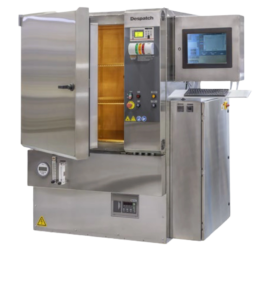 One noteworthy example in the world of curing ovens is the Despatch PCO2-14™ Polymide Curing Oven, a high-performance, clean process oven designed specifically for polyimide baking and curing applications. This electrically heated oven meets the specific process requirements for hard baking polyimide coatings in an inert atmosphere. Its ISO Class 5/Class 100 recirculated airflow, pressure relief system, oxygen control system, and process monitoring system allow it to achieve the strict oxygen levels and atmospheric requirements involved in polyimide curing.
The Despatch PCO2-14™ and ovens like it are essential tools in semiconductor manufacturing, ensuring the reliability and functionality of electronic devices through precise temperature control and a controlled environment. They not only meet the demands of polyimide curing but also play a pivotal role in a wide range of semiconductor packaging applications, making them indispensable in the ever-evolving world of electronics.